A team at Lawrence Berkeley National Laboratory has just announced a new breakthrough in the field of graphene research, leading to the next generation of high-efficiency solar cells, computers and other advanced technologies. Graphene, a new material that was discovered less than 10 years ago, is an ultra-thin, superstrong, superflexible electron conductor. As for how to explain the Berkeley Lab research in lay terms, let’s just say that if graphene had a personality it would have its own reality show, and it would give Total Divas a run for the money.
No, seriously. Researchers have already demonstrated that graphene possesses an outsized talent for showing off its unique properties, which is surely one prerequisite for diva-ness. The other is a highly developed sensitivity to minor irritations, and that is the focus of the new Berkeley Lab research.
A Graphene Mystery
To understand the significance of the Berkeley Lab breakthrough, let’s start at the beginning. Graphene consists of a sheet of carbon only one atom thick, with a distinctive lattice structure similar to chicken wire.
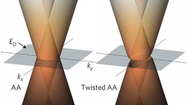
Dirac spectrum in bilayer graphene courtesy of LBL.
On the plus side, graphene is an extremely efficient conductor, far more efficient than silicon. However, this is where graphene’s diva side kicks in. To translate graphene into on/off devices, you need to be able to switch off the conduction, and graphene simply refuses to shut itself down completely.
The basic problem is that a single sheet of graphene has no range of energy that prohibits electrons from existing. Called a bandgap, this range is essential for controlling the electron current.
Berkeley Lab researchers previously attempted to work around the problem by using two layers of graphene to create a bandgap. However, when the bilayer graphene was incorporated into devices it flopped. The devices acted as if the graphene was a single layer, with no bandgap.
Mystery, Solved!
Picking apart that phenomenon is the next critical phase in the research, and that is where the new Berkeley Lab research project comes in.
Using the Lab’s Advanced Light Source, they subjected the bilevel graphene to a beam of X-ray photons. That analytic tool produces a snapshot of the material’s electronic spectrum.
The results were surprising. In contrast to what the team had assumed, the spectrum contained extra branches. These consisted of massless Dirac fermions, which are electrons that behave like photons (named after U.K. physicist Paul Dirac). Since Dirac fermions do not follow the same bandgap rules as normal electrons, that explains why the bilayer graphene had no “on-off” switch.
The team traced the creation of massless Dirac fermions to atomic-level misalignments between the two layers of graphene. While almost imperceptible, the misalignment creates a “twist” in the material that generates the massless Dirac fermions.
The bad news is, the problem is not easily resolved. The team estimates that just ten atomic “misfits” per square micron are enough to throw the whole thing off.
However, the team anticipates that the results will guide it to the next step in the research. Lead author of the study Keun Su Kim explains:
Now that we understand the problem, we can search for solutions. For example, we can try to develop fabrication techniques that minimize the twist effects, or reduce the size of the bilayer graphene we make so that we have a better chance of producing locally pure material…
Kim also sees the study applying across the field of graphene research:
A lesson learned here is that even such a tiny structural distortion of atomic-scale materials should not be dismissed in describing the electronic properties of these materials fully and accurately.
More Exciting News About Graphene
As mentioned above, graphene has only been around since 2004, when a U.K. research team literally lifted a layer of atoms from the surface of a chunk of graphite with sticky tape, but the topic has already generated thousands of research papers as scientists race to unlock the mysteries of its unique properties.
Among the many recent developments, researchers are beginning to identify materials that mimic graphene’s more desirable properties, while being more capable of taking direction and put up with minor irregularities. A team at Columbia University, for example, used boron nitride (aka “white graphene”) to create the rare “Hofstadter butterfly” fractal pattern (a fractal pattern repeats itself in smaller and smaller shapes).
A research team in Spain went even farther afield, finding that they could develop an acoustic analog for graphene simply by drilling holes in a sheet of plastic.
As for why CleanTechnica is so interested in graphene (see our numerous posts on the topic), photovoltaic cells are among the many devices that could be looking at an ultra-efficient graphene future.


